FM Transceiver
This project was made for the Electronics Engineering program at Okanagan College in 2022. The idea was to integrate digital control architecture with RF components to create a low power 2-way FM radio (pair of walkie talkies); Below is a technical description of the project.
| Project | FM Transceiver Pair (two devices) |
|---|---|
| Program / Year | Electronic Engineering Technology, 2022 (Okanagan College) |
| Modulation | FM (Frequency Modulation) |
| Target Range | 10 m (indoor short-range) |
| Battery | Single 18650 Li-ion (3000 mAh) |
| Standby Time (spec) | 3 hours |
| Continuous TX Time (spec) | 30 minutes |
| MCU | Microchip PIC24FJ1024GB606 |
| RF Transceiver | Silicon Labs SI4720 (76–108 MHz band) |
| Audio Output | 8 Ω speaker + TI TPA321 amplifier (BTL) |
| Display | 1.3" SPI GLCD (Adafruit 4313, 240×240, ST7789 controller) |
| Battery Protection | TI BQ77905 (“BATMAN”) + NTC + dual MOSFET cutoff |
| Battery Monitoring | MCP3021 (10-bit I²C ADC) + buffer stage |
| Status | Not fully functional (SPI timing/transfer issues prevented control of SI4720 + GLCD) |
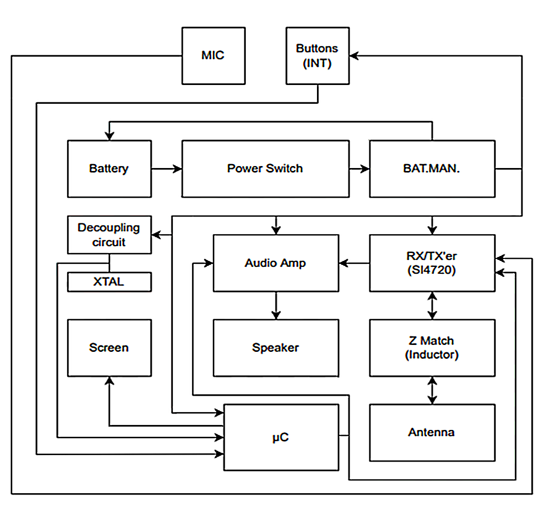
Battery management
The power supply block provides energy to the system and ensures safe battery operation. It includes the battery cell, a master disconnect switch for complete power isolation, and a battery management circuit that protects the cell and disconnects it under fault conditions.
System inputs
The system input block provides the primary user interface and power control for the device. It includes the microphone for audio input, user buttons for device control, and a main power switch that connects or disconnects the battery.
MCU support
The MCU support block contains the circuitry required for stable and reliable microcontroller operation. It includes decoupling capacitors that filter supply noise and stabilize the MCU power rails, as well as a crystal oscillator that provides the system clock.
Outputs
The system output block includes the display and audio output components. A 1.3-inch screen presents key system information. Audio output is provided through a speaker driven by a dedicated amplifier.
Audio amplifier
The audio amplifier block boosts the received audio signal to a level suitable for driving the speaker.
Microcontroller
The MCU acts as the central controller for the system, handling user inputs, managing operating modes, and coordinating communication between the RF backend, display, and audio output.
RF backend
The RF backend is responsible for all wireless communication within the system. A single transceiver IC handles both transmit and receive operation, simplifying the overall RF architecture. Carefully selected matching components are used to ensure proper impedance matching and efficient RF performance.
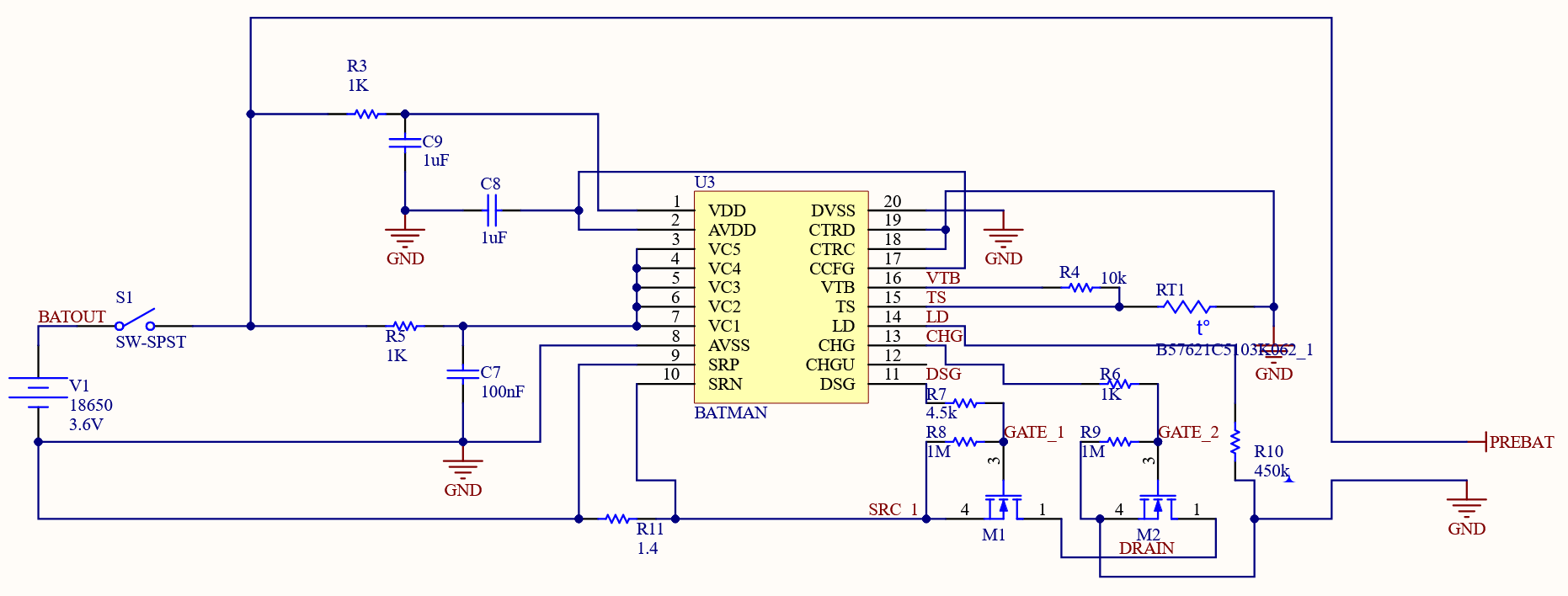
The BATMAN battery management subsystem is built around the Texas Instruments BQ77905 battery manager and is responsible for safely managing a single 18650 Li-ion cell. Its primary role is to protect the battery by providing over-voltage, under-voltage, over-current, short-circuit, and temperature protection. The BATMAN IC continuously monitors cell voltage, charge and discharge current through a sense resistor, and cell temperature using an external NTC thermistor. When unsafe conditions are detected, the device drives two external MOSFETs to disconnect the battery from the system load. Status signals such as CHG, DSG, and LD give the system controller real-time insight into battery and load conditions. Within the overall design, this subsystem forms the core of the power supply, ensuring user safety and protecting all downstream electronics. By isolating fault conditions at the battery level, BATMAN improves system reliability and allows the transceiver to operate safely from a removable high-energy Li-ion cell.
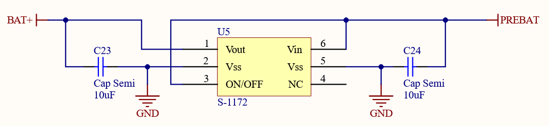
The S-1172 voltage regulator stage is used to condition battery power for the rest of the system. It takes the protected battery output (PREBAT) and generates a stable, regulated supply rail for the downstream digital and RF electronics. Input and output capacitors are placed close to the device to ensure regulator stability, suppress noise, and handle transient current demands. The ON/OFF control pin allows the regulator to be cleanly enabled or disabled as part of the system power-up sequence. By regulating the inherently variable voltage of a single 18650 Li-ion cell, this stage helps prevent brownouts and over-voltage stress on sensitive components. In the overall design, this block sits directly after the BATMAN battery manager and serves as the final power-conditioning step, ensuring reliable operation across the full battery discharge curve.
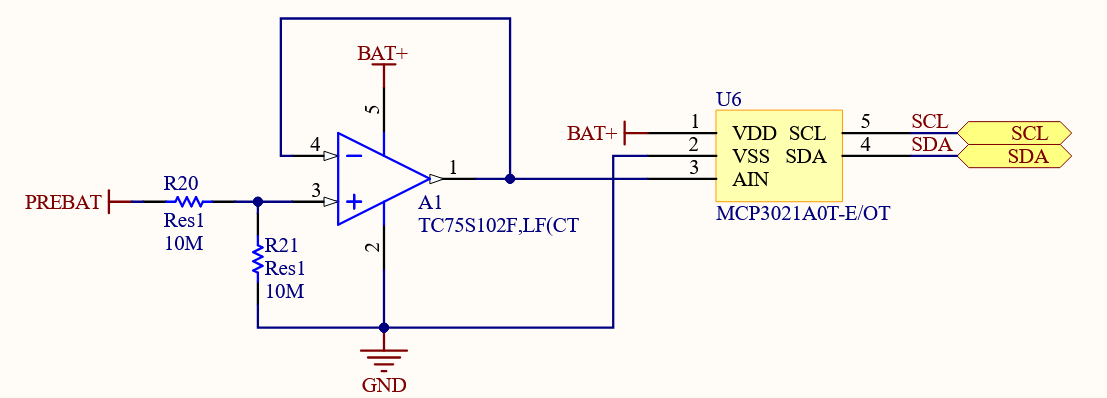
The battery voltage monitoring circuit measures the protected battery rail and provides a low-power way for the microcontroller to estimate remaining charge. A high-value resistor divider is used to scale the battery voltage while keeping continuous current draw to a minimum. The divided signal is buffered using a TC75 op-amp, which presents a stable, low-impedance output that isn’t affected by ADC loading. This buffered voltage is then digitized by the MCP3021 I²C ADC. Using a dedicated ADC allows the microcontroller to periodically sample the battery voltage without directly loading the battery or sensitive analog node. In the overall system, this block supports battery percentage estimation and low-battery warnings while maintaining good power efficiency.
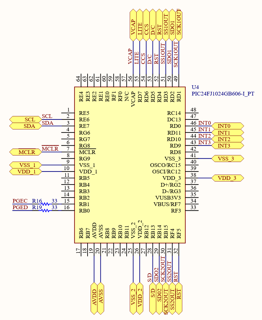
The microcontroller serves as the central controller for the system, handling high-level logic, coordination between subsystems, and all user interaction. It communicates with peripherals over SPI and I²C, processes external interrupts from user inputs, and manages system states such as transmit/receive operation, display updates, and power behavior. Separate power and ground pins are used to help isolate digital and analog domains and reduce noise sensitivity. Firmware programming and debugging are supported through dedicated ICSP connections. By relying on interrupt-driven inputs rather than continuous polling, the system remains responsive while minimizing processor overhead. In the context of the full design, the microcontroller ties together the RF, power management, audio, and user interface subsystems.
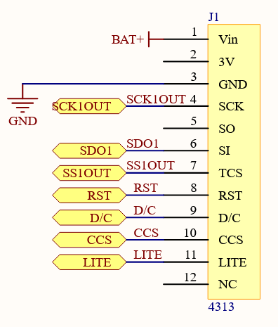
The graphical LCD serves as the primary visual interface for the device, presenting system status and user feedback during operation. It is powered directly from the system supply and communicates with the microcontroller over an SPI interface. Dedicated control lines manage reset, data/command selection, chip select, and backlight control, allowing the display to be updated efficiently and flexibly. The backlight enable line provides the option to adjust brightness or disable the backlight entirely to save power when the display is not in use. Within the overall system, this module functions as the main user interface, displaying information such as battery level, operating mode, and channel selection.
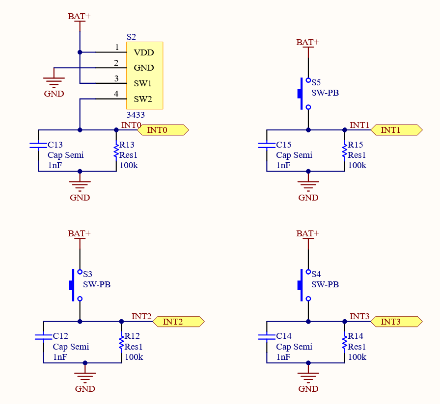
The input and interrupt circuit handles all user button interactions and converts them into clean, reliable digital signals for the microcontroller. Each pushbutton is biased from the battery rail and uses an RC network to debounce the mechanical switch action. The conditioned signals are routed directly to dedicated external interrupt pins, allowing the system to respond immediately to user input rather than relying on continuous polling. A dual-switch device is used to reduce component count while still maintaining independent inputs. This approach lowers processor overhead and improves responsiveness. In the context of the full system, this block enables smooth and reliable user control for mode selection, adjustments, and transmit/receive operation.
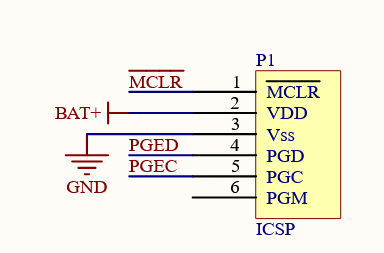
The ICSP programming interface allows the microcontroller to be programmed and debugged directly on the board without needing to remove it from the circuit. It brings out the necessary power, ground, reset, and programming data and clock lines needed for in-circuit programming. This makes firmware updates, debugging, and recovery much easier during development and testing. The interface follows Microchip’s standard ICSP pinout, ensuring compatibility with common programming tools. Keeping this header on the board simplified iteration and troubleshooting throughout the project, and it serves as the critical link between firmware development and the physical hardware.
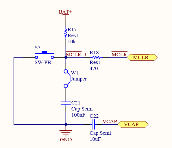
The reset and startup circuit ensures the microcontroller always powers up in a known, stable state and can be reliably reset by the user when needed. A pull-up resistor holds the reset line high during normal operation, while a pushbutton allows the reset line to be asserted manually. An RC network adds a short delay during power-up to prevent false resets while the supply voltage is ramping. A series resistor helps protect the reset pin and improves signal integrity. A jumper is included to provide flexibility during development and troubleshooting by allowing the reset behavior to be modified. Together, this circuitry ensures predictable startup behavior and reliable recovery from fault conditions.
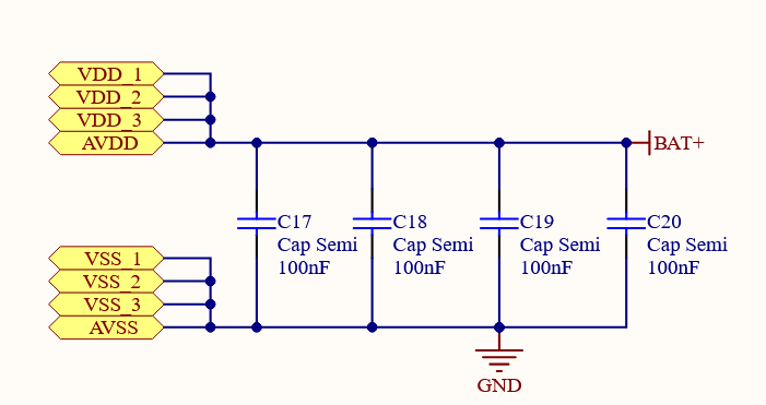
The power decoupling network stabilizes the supply rails that feed both the digital and analog sections of the system. Local bypass capacitors provide a low-impedance path to ground for high-frequency noise and short current spikes caused by switching activity. Separating the VDD and AVDD domains helps prevent digital noise from coupling into more sensitive analog circuitry, improving overall signal quality. By placing the decoupling components as close as possible to the load, disturbances are filtered before they can spread across the board, reducing the chance of erratic behavior or unintended resets. In the context of the full design, this block is critical to the reliable operation of the microcontroller and other mixed-signal components.
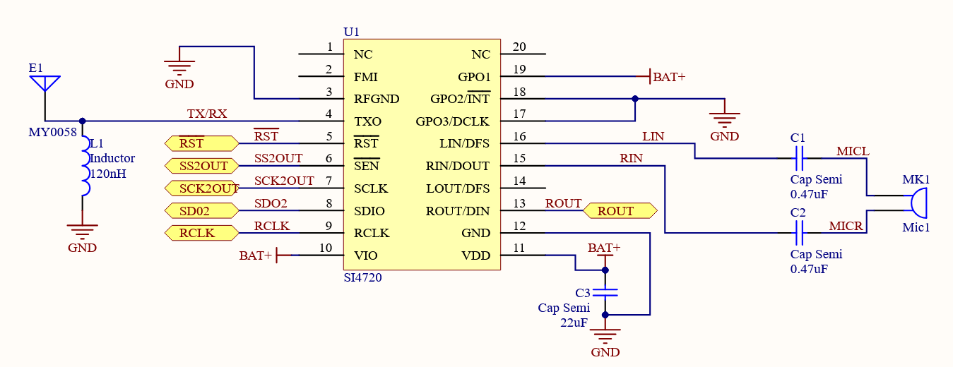
The FM transceiver block is responsible for all wireless transmit and receive functionality, as well as interfacing the audio signals used by the system. The SI4720 integrates modulation, demodulation, and RF signal processing into a single device, which helped reduce both external component count and overall RF design complexity. An external antenna, along with a matching inductor, forms the RF front end to support efficient transmission and reception. The microcontroller communicates with the transceiver over a serial interface, allowing the operating frequency, mode, and power settings to be configured in software. Audio from the microphone is AC-coupled into the transceiver, while received audio is routed to the downstream amplifier. As a whole, this block acts as the core communication engine that enables two-way FM voice operation.
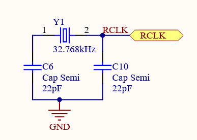
The crystal oscillator supplies a stable reference clock for the transceiver’s internal timing and frequency generation. A 32.768 kHz crystal, paired with matched load capacitors, is used to ensure reliable startup and long-term frequency stability. This low-frequency reference enables consistent tuning and repeatable RF performance. Careful grounding and symmetric loading were used to reduce phase noise and avoid startup issues. In the overall system, this clock source isi>s foundational to accurate modulation, demodulation, and channel stability.
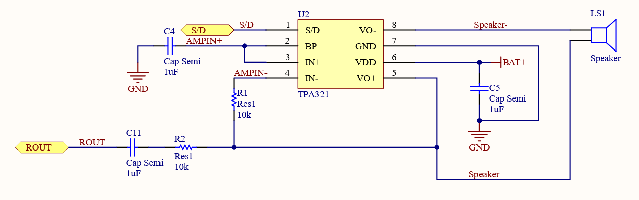
The audio amplifier stage takes the low-level audio output from the transceiver and boosts it to a level suitable for driving the speaker. The TPA321 is configured in a bridge-tied load arrangement, allowing higher output power from a low supply voltage without the need for a large coupling capacitor. Input coupling and biasing components condition the signal and remove any DC offset before amplification. Local decoupling is used to keep the amplifier stable under changing audio loads. A shutdown control line allows the amplifier to be disabled when audio output isn’t needed, helping reduce overall power consumption. In the system as a whole, this block translates the demodulated RF signal into clear, audible sound for the user.
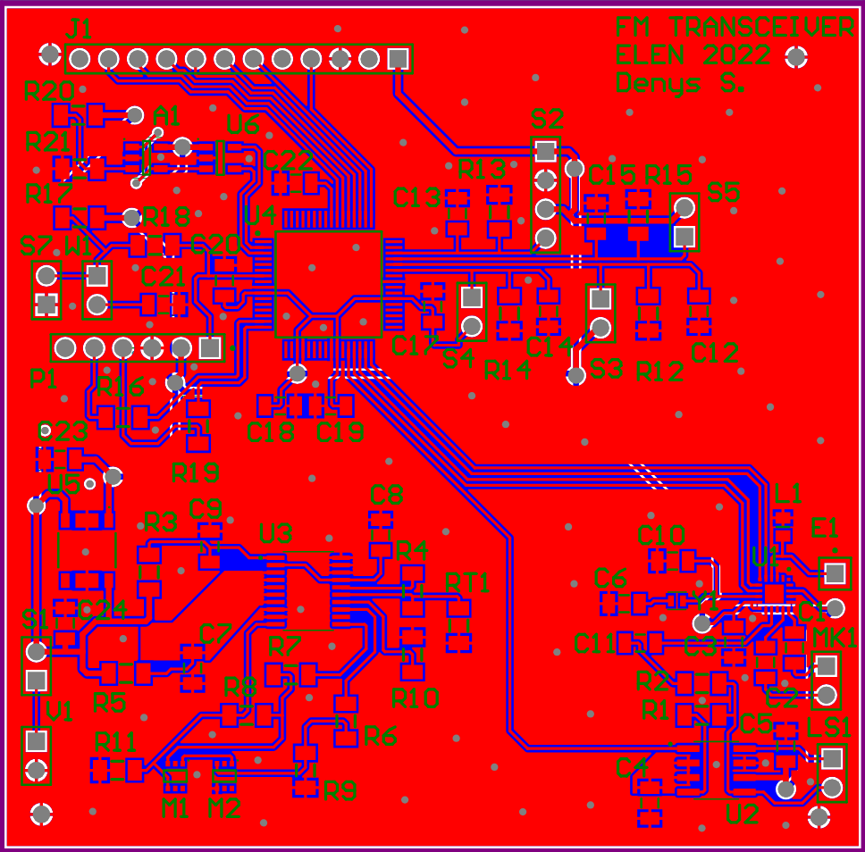
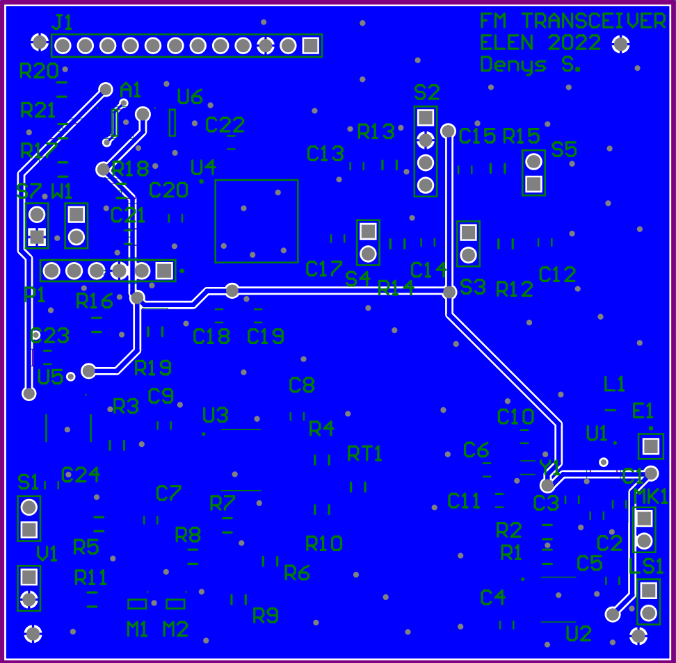
The PCB layout was approached with functional partitioning and signal integrity as primary goals. Components were grouped by subsystem—such as MCU support, RF front end, audio, and power management—to keep routing logical and reduce trace lengths for sensitive signals. High pin-count devices were placed centrally to simplify fan-out and reduce routing congestion, while decoupling capacitors were positioned as close as possible to IC power pins to help control supply noise. A continuous ground reference and short return paths were maintained across the board to improve overall stability and robustness.
The RF transceiver was intentionally placed in the bottom-right corner of the PCB, close to the antenna connection point (E1). Positioning the RF section near the antenna minimized the length of sensitive RF and small-signal traces, reducing the chance of noise coupling from digital logic and power circuitry elsewhere on the board. Localizing the RF components also made impedance-aware routing more straightforward and helped keep the antenna interface clean and predictable.
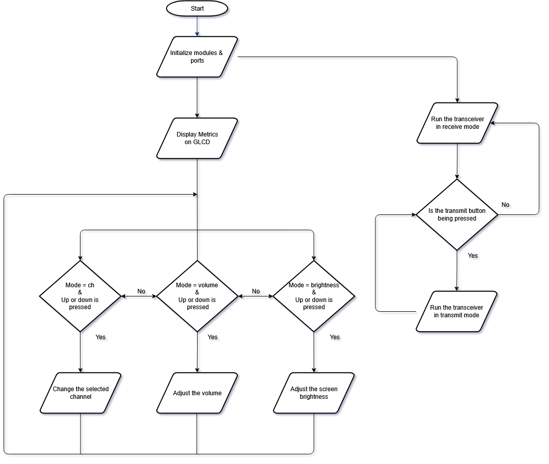
On startup, the system initializes all hardware modules and I/O lines, then brings up the graphical LCD to show the current operating state. During normal use, the radio stays in receive mode and continuously listens for user input. The selected mode determines what the up and down buttons control, allowing the user to switch channels, adjust the audio volume, or change the display brightness. When the transmit button is pressed, the system briefly switches into transmit mode and automatically returns to receive once the button is released. This loop runs continuously, allowing the device to respond quickly and predictably to user interactions.
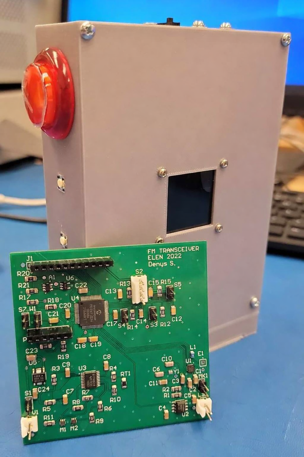
Physical assembled prototype.
Interactive Fusion 360 enclosure design.
This project was a major learning experience for me and involved several first-time milestones in both hardware and mechanical design. It was my first time assembling a PCB using a reflow oven, with most of the passive components soldered by hand, which forced me to be deliberate about placement, inspection, and rework. I also designed a custom enclosure in CAD for the first time, learning how mechanical constraints, board geometry, and connector placement all have to work together in a real device. While the system was not fully functional in its final state, the failure was traced back to a timing issue in my SPI library that prevented the SI4720 transceiver from initializing correctly—specifically, incorrect clock polarity and setup timing during early configuration commands. Debugging this exposed how sensitive RF ICs can be to low-level digital timing and reinforced the importance of validating firmware assumptions against datasheet requirements. Through this project, I developed a much stronger understanding of RF-aware PCB layout, power integrity, decoupling, and subsystem partitioning, as well as practical experience diagnosing problems that span firmware, digital interfaces, and analog RF hardware.